The initiative leverages a collaborative ecosystem involving partners such as Neitas, Daikin, BlueDot Ventures, FMC, and Advanced Printed Electronic Solutions (APES). By utilizing the FINPAT packaging technology, the team aims to create additively manufactured substrates that house heterogeneous semiconductors alongside multiple specialized sensors. This approach allows for the direct integration of GLS power management, RISC-V processor chips, and FMC ferroelectric memory into a unified, energy-efficient module.
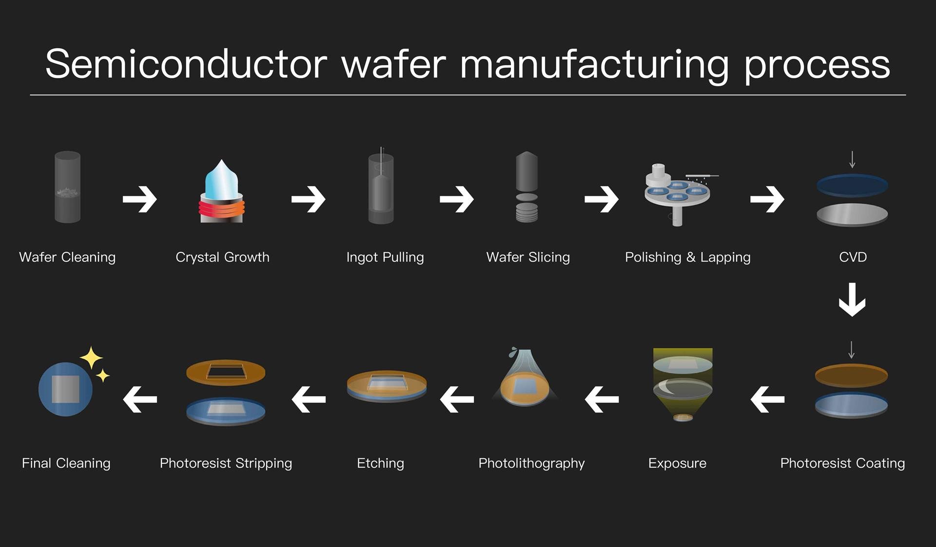
At the core of this operation is the ChipForge platform, a modular wafer-fabrication system designed to support diverse semiconductor processes without requiring the wholesale redesign of conventional facilities. According to GLS Chairman and CEO Dr. Richard Thurston, the model aligns manufacturing blueprints from the design phase, allowing for rapid iteration of prototypes. APES CEO Dr. Rich Neill noted that the system enables engineers to adjust design parameters and generate new prototypes without developing entirely new materials or rules. By embedding energy harvesting and printed electronics directly into the packaging, the collaboration seeks to produce AI-driven sensors that retain machine-learning data with minimal power consumption, effectively creating a new standard for high-performance, compact hardware.



Comments (0)
No comments yet. Be the first!